International Journal of Electrical and Computer Systems (IJECS)
ISSN: 1929-2716

Volume 4, Year 2018 - Pages 1-5
DOI: 10.11159/ijecs.2018.001
Design and Fabrication of Stepped Impedance Multi-Function Filter
Rajinikanth Yella, Krishna Pande, Ke Horng Chen, Li-Chun Wang
National Chiao Tung University, Department of Electrical Engineering
No. 1001, Daxue Road, East District, Hsinchu City, 300, Taiwan
rajini.02g@g2.nctu.edu.tw; kppande@nctu.edu.tw; krimaps@gmail.com; lcwangnctu@gmail.com
Abstract - This paper presents the design and fabrication of multifunction filter with compact size, low loss and high selectivity. The basic building block of the multifunction filter is based on an optimized stepped-impedance low pass filter (LPF) circuit using microstrip line. The LPF circuit can be modified with minor changes to make it a Band Pass (BPF) and High Pass filter (HPF). For BPF, a simple matching network is added at the output of LPF. Addition of matching network does not contribute significant loss as evident from the value of return loss, typically -20 dB at 5.8 GHz. For creating HPF, all shunt stubs of the same LPF are connected to the ground. The proposed Filters were fabricated on FR4 to validate the design concept with a goal of transferring the design to GaN substrate for on-chip transceiver application. Our measurement results show excellent agreements with simulated results. To our knowledge, design of such multifunction filter has not been reported. Our filter provides SWAP-C advantages.
Keywords: Multi-function Filter, Micro-strip line, Stepped impedance filter.
© Copyright 2018 Authors - This is an Open Access article published under the Creative Commons Attribution License terms. Unrestricted use, distribution, and reproduction in any medium are permitted, provided the original work is properly cited.
Date Received: 2017-11-27
Date Accepted: 2018-04-18
Date Published: 2018-05-01
1. Introduction
Filters are an essential part of wireless communications systems as they are required to suppress undesired signals in the transceiver. The size, weight, and power plus cost and loss of such filters must be kept as low as possible. Currently, separate filters, such as low pass, band pass and high pass, are used to suppress unwanted signals depending upon system requirements. However they are designed and integrated separately increasing SWAP-C. Hence, there is critical need for multifunction filter, which can be integrated on-chip to support multiband operation [1] of a transceiver. Thus current trend in filter design is to focus on reducing SWAP-C, creating filters on chip and use low loss materials such as artificial meta-materials as reported previously [2-4].
Stepped-impedance structure has been typically used to implement microstrip based Low pass filters (LPFs) by cascading very high and very low characteristic impedance transmission lines alternately [5]. Increasing circuit order can improve the filter performance but may lead to increased insertion loss and unacceptable circuit size. To overcome this problem, a number of methods have been proposed such as defected ground structure (DGS) and series of grounded patches (SGP) [6, 7]. In this paper, a unique technique, that involves adjusting the structure parameters of each pole/line section of filter, is proposed to make stepped impedance filter as multifunction filter. In our design varying the structure parameters of each pole such as, attenuation poles are achieved leading to low insertion loss and high return loss of proposed filter.
In this paper, design of a core circuit using microstrip line has been conceived and designed that works as LPF. This core circuit with minor changes is converted into multi-function BPF and HPF. For BPF a simple matching network is added at the output of LPF. Addition of matching network does not contribute significant loss as evident from the value of S11. For HPF, same LPF circuit is reconfigured by grounding all shunt stubs. Advanced Design System (ADS) software has been used to design the proposed filter at a microwave frequency (5.8 GHz) but design is applicable at millimeter-wave frequencies too. In order to prove the validity of our design, the proposed Filters were fabricated/implemented on FR4 with a dielectric constant of 4.4, a substrate thickness of 1.6 mm and a loss tangent of 0.02. It has an overall dimensional of 46.6 mm by 6.6 mm. Both simulation and measurement results are presented and discussed. Our measurement results show excellent agreements with simulated results.
2. Design and Optimization of Multi-Function Filter
2.1. Low Pass Filter
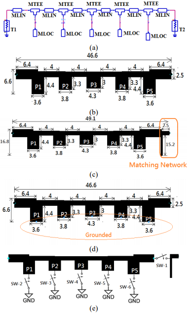
In our design, width and lengths of line sections of stepped impedance filter are optimized to create a multifunction filter. The Fig 1(a) illustrates, an optimized stepped-impedance microstrip line based design of the proposed LPF. We used micro-strip line (MLIN), microstrip open-circuited stub (MLOC) and micro-strip T junction (MTEE) to design the filter circuit. Its layout is presented in Fig 1(b) with a total of 5 poles. In our proposed filter concept, number of poles decides range of cut-off frequency of a filter. For example we designed LPF circuit with cut-off frequency of 5GHz, therefore, we placed 5 poles. To enhance attenuation in the stop band, length and width of the poles of proposed filter are adjusted. P1 and P5 are identical as well as P2 & P4 are identical in length and width. Length of P1or P5 > length of P2 or P4 > length of P3. Whereas the Width of poles should be such that width of P3> width of P2 or P4 > width of P1 or P5. For microstrip filters optimum distance between poles is also very crucial as this length will act as capacitive or inductive (depending upon the frequency of operation and distance between poles). The passband frequency could be adjusted via the structure parameters of the poles. The designed multifunction filter is simple in structure and compact in size.
2.2. Band Pass Filter
Traditionally matching networks based on spiral inductors are preferred instead of resistors. However, their use at high frequencies is limited due to self-resonance and stray impedances. In addition, they occupy large space on the chip. In order to overcome this problem, we designed an L-type matching network using stubs as shown in Fig 1(c). Proposed BPF layout is shown Fig. 1(c). As mentioned above, LPF circuit with minor changes behaves like BPF. For BPF a matching network is added at the output of LPF. Addition of matching network does not contribute significant loss as evident from the value of S11 (lower than-o.20). The BPF passband at the desired frequency is realized by adjusting the structural parameters of the matching network. For ADS simulation of BPF circuit, we placed Via-ground instead of normal ground. As a results, ADS simulation gives almost same performance as measured results.
2.3. High Pass Filter
Traditionally HPF circuit design consists of shunt inductors. According to Richards’s [8] transmission short-circuited stub behaves like inductor. Hence we grounded all shunt stubs of same LPF, as a result it behaves like HPF and its corresponding layout is shown in Fig1 (d). By the use of 6 switches as shown in Fig 1(e), our proposed design can operate in any mode (LPF or BPF or HPF). If switch 1 is connected, LPF acts as BPF. If switches 2-6 are connected LPF acts as HPF.
2.4. Fabrication
The proposed Filters were fabricated on FR4 with a dielectric constant of 4.4, a substrate thickness of 1.6 mm and a loss tangent of 0.02.It has an overall dimensional size of 46.6 mm by 6.6 mm. Fig 2 shows top view of fabricated filters, as proposed.
3. Results and Discussion
The simulated and measured results for S11 and S21 of proposed LPF, BPF and HPF are shown in Fig 3. Our measurement results show excellent agreements with simulated data from ADS. Here S21 parameter represents the transmission line characteristics and the S11 parameter represents the return loss characteristics.
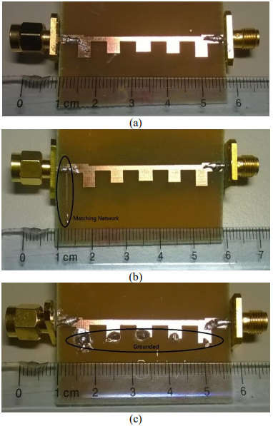
Fig 3(a) depicts response of proposed LPF. In case of LPF, simulated -3 dB passband range is obtained from DC to 5.2 GHz. From DC to 3.1 GHz the insertion loss is less than -0.4 dB and the return loss is better than -38 dB. One attenuation pole is at 6.4 GHz. The simulation and measurement have a difference of less than 0.1dB in insertion loss, less than 5 dB in return loss at the passband DC-5GHz.
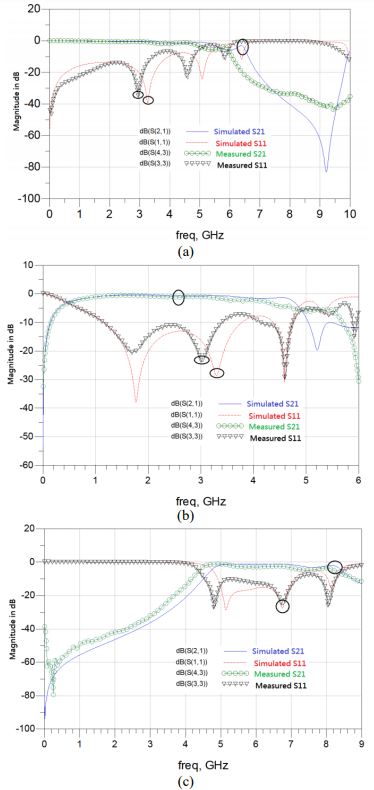
Fig 3(b), presents simulated and measured response of proposed BPF. In case of BPF, measured insertion loss is -3 dB over a bandwidth of 0.47 GHz to 4.7 GHz. The best match for the BPF is obtained at 3.11 GHz. The center frequency of pass band is 2.46 GHz. BPF has insertion loss less than -0.3 dB and return loss greater than -28 dB over 1.3 GHz to 3.3 GHz as shown in fig 3(b). It is also observed that the insertion loss drops sharply outside of the passband that indicates a high selectivity. The simulation and measurement have a difference of less than 0.2dB in insertion loss, less than 5 dB in return loss at the passband (0.5-4.2GHz).
Fig 3(c), illustrates response of proposed HPF. In case of HPF -3 dB bandwidth is obtained over 4.8 GHz to 7.8 GHz. HPF has insertion loss less than -0.2 dB and return loss greater than -26 dB at 6.7 GHz frequency as shown in Fig 3(c). One attenuation pole occurred at 6.4 GHz. The simulation and measurement have a difference of less than 0.1dB in insertion loss, and less than 1 dB in return loss at the passband (4.8-7GHz).
We have simulated our multifunction filter circuits with built-in VCS (voltage controlled switch) switches. The results are plotted in fig 3 for BPF and HPF including switch losses which are acceptable. Slight difference between the simulated and experimental results may be due to devive dembedding, reflection, signal attenuation from SMA and losses from wire bonds etc in case of experimental data. In addition process variation has some effect too.
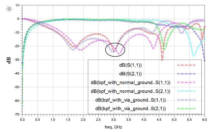
The simulated performance of filter circuits can be achieved with both normal ground and via ground. However, we have used via ground for simulating the circuit in order to obtain S-parameter results compatible with measured data. PCB used in our experiment is a two-layer structure with filter circuit fabricated on top layer and metalized bottom layer used as ground. Metalized via holes connect the elements on top layer. In case of BPF and HPF, some microstrip lines are connected to ground. While using via ground in ADS simulation, we can inputted the values of substrate thickness and via-hole diameter, as related to normal ground and via ground simulation for BPF (Fig. 4).
A comparison of simulated and measured performances of the proposed multifunction (LPF, BPF and HPF) is highlighted in Table I. Attenuation poles are achieved by varying the structure parameters of each pole, which offers more freedom for design. Thus, this design method is very flexible for configuration and especially useful to get low insertion loss and high return loss. A comparison of performance of the proposed work (LPF, BPF and HPF) with previously published work (LPF and BPF) using lumped elements [9] is highlighted in Table 1. We conclude that our results are better than previously published results [9-11]. The filters reported in this paper can operate in any mode (LPF or BPF or HPF) using a bank of 6 low loss switches such as [11].
Table 1. Design Specifications of Simulated and Measured.
| Key Parameter | Proposed | [6] | [7] | ||||||
| LPF | BPF | HPF | LPF | BPF | BPF | ||||
| Sim | Mea | Sim | Mea | Sim | mea | ||||
| 3 dB band (GHz) | 0 to 5.2 | 0 to 5 | 0.46 to 4.7 | 0.5 to 4.2 | 4.8 to 7.8 | 4.4 to 7.0 | 2.5 | 2.5 | 2.17 |
| IL, (dB) | <-0.4 | <-0.5 | <-0.3 | <-0.5 | <-0.2 | <-0.3 | <-0.8 | < 1.2 | <-2.1 |
| RL, (dB) | >-38 | >-33 | >-28 | >-23 | >-26 | >-25 | >-13 | >-12 | >-29 |
*Sim-Simulated, Mea-measurement, IL- Insertion loss, RL-return loss
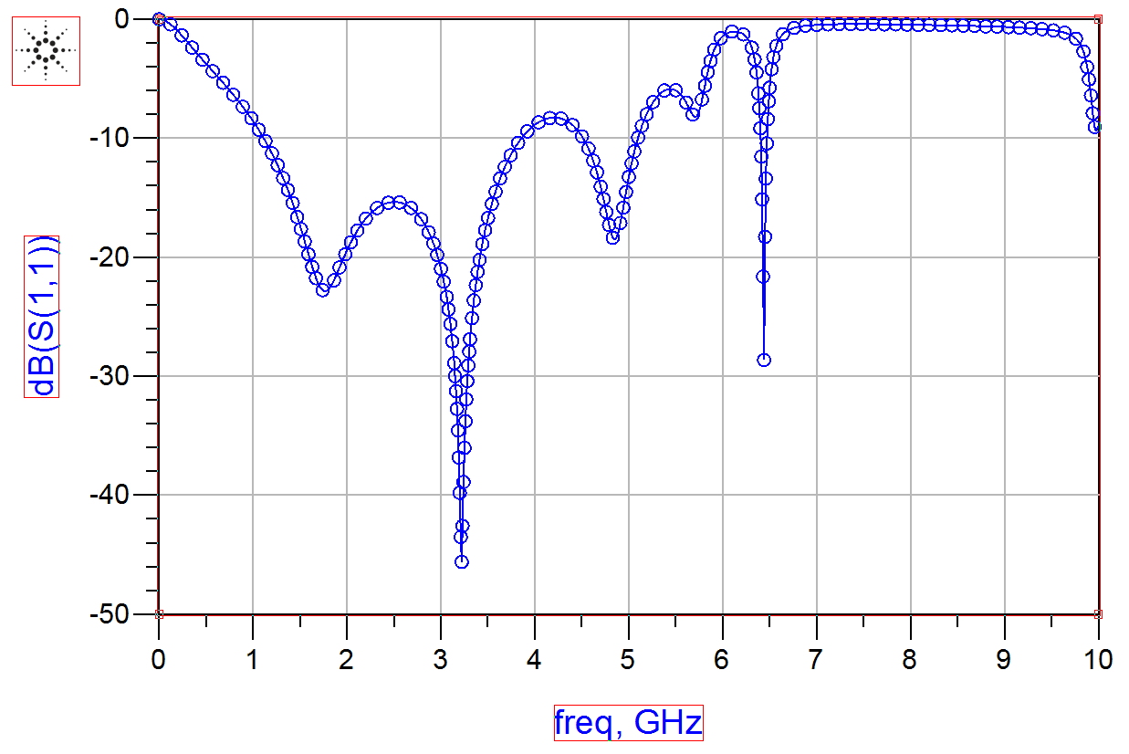
To investigate the loss of multi-function filter with six switches, we simulated end to end S11 in ADS. The results are shown in Fig.5. Traditionally S11 is calculated to check loss value of circuit. The S11 value at pas-band frequency is lower than -10dB.
4. Conclusion
A new core LPF circuit is proposed that with minor modifications performs as a BPF and HPF. Novelty of our paper involves addition of a simple matching circuit which can transfer LPF into BPF and HPF without adding much losses. We have not seen such filter design published so far. Our filter technology offers excellent SWAP-C advantages and eliminates losses due to multiple filter packages and wire bonds. Further, channelization for isolation is not needed. Proposed multifunction filter can be used for on-chip RF transceivers. The design and fabrication of optimized stepped impedance multifunction filter high isolation and high selectivity is presented. The design procedure is simple and it can be easily and inexpensively fabricated on-chip (such as GaN) or common printed circuit board (such as FR4) technology. The filters reported in this paper can operate in any mode (LPF or BPF or HPF) using a bank of 6 low loss switches. No such design concept has been reported to our knowledge.
Acknowledgment
Authors would like to thank National Chiao Tung University, Taiwan for providing the research facilities available in the Electrical Engineering Department.
References
[1] S. L. Yo, C. L. Chien, M. L. Ko, H. C. Chun, “Design of an LTCC Tri-Band Transceiver Module for GPRS Mobile Applications,” IEEE Transactions on Microwave Theory and Techniques, vol. 52, pp. 2718-2724 2004. View Article
[2] M. Palandoken, A. Sondas, “Compact Metamaterial Based Band-Stop Filter,” Microwave Journal, vol. 57, no. 10, pp. 76-84, 2014. View Article
[3] M. Palandoken, M. H. B. Uçar, “Compact Metamaterial-inspired Band-Pass Filter,” Microwave And Optical Technology Letters, vol. 56, no. 12, pp. 2903-2907, 2014. View Article
[4] M. Palandoken, “Metamaterial-Based Compact Filter Design,” Metamaterial, Dr. Xun-Ya Jiang (Ed.), 2012. ISBN 978-953-51-0591-6 View Article
[5] M. Jiang, W. Hong, “An Approach for Improving the Transition-band Characteristic of a Stepped-Impedance Low-Pass Filter,” ICMMT International Conference, 2012. View Article
[6] P. S. Kiran, P. Anurag, D. U. Madhur, “Novel Approach for Loss Reduction in LPF for Satellite Communication System,” IACC International Conference, 2013. View Article
[7] M. Kadota, M. Esashi, S. Tanaka, Y. Ida, T. Kimura, “Improvement of Insertion Loss of Band Pass Tunable Filter using SAW Resonators and GaAs Diode Variable Capacitors,” IUS International Conference, 2013. View Article
[8] D. V. George, M. P Anthony, L. R Ulrich, Microwave Circuit Design Using Linear and Nonlinear Techniques, 2nd ed. New Jersey and Canada: John Wiley, 2005, pp. 297-298. View Book
[9] D.-H. Kim, D. Kim, J.-C. Kim, J.-C. Park and C.-D. Park, “Design of selectable low- and bandpass filter for 2.4 GHz applications,” IEEE Electronics Letters, vol. 46, pp. 1699-1700, 2010. View Article
[10] W. T. Koh and K. M. Lum, “Dual-band Bandpass Filter Design Using Stub-loaded Resonators,” IEEE Progress in Electromagnetics Research Symposium Proceedings, Russia, vol. 4, pp. 1491-1494, 2012.
[11] Y.-H. Cho, H.-I. Baek, H.-S. Lee, and Sa.-W. Yun, “A Dual-Band Combline Bandpass Filter Loaded by Lumped Series Resonators,” IEEE Microwave and Wireless Components Letters, vol. 19, pp. 626-628, 2009. View Article
[12] B.-W. Min, and G. M. Rebeiz, “Ka band low loss and high isolation switch design in 0.13 um CMOS,” IEEE Transactions on Microwave Theory and Techniques, vol. 56, pp. 1364-1371, 2008. View Article